Smaller scale, greater efficiency
The subject matter of Chou’s “Atomic-Scale Variability and Control of III-V Nanowire Growth Kinetics” may seem a bit abstruse, but nanoscale components are already a fact of life in everyday items such as computers and cellphones.
Chou explains that pushing the state of the art into nanoscale technology allows components to be packed more closely together on semiconductor wafers, which increases their efficiency and may well lead to next-generation technologies in the semiconductor, computing, and biomedical device industries.
Chou works on “III-V group” materials, which are compounds formed from the Group III and Group V elements on the periodic table of elements (there are eight groups in total).
She says that at the same width, wires made from Group III-V materials have higher electron mobility and waste less power than those made from Group IV materials. Scientists have been researching these materials in recent years in the hope that they will eventually replace silicon in semiconductors. The gallium phosphate (GaP) Chou studies is a case in point.
Currently, most nanowires are manufactured via lithographic processes that involve etching pathways into a substrate. With self-assembly, atoms instead form themselves into nanowires by deposition.
“Lithography is already at its limit. Self-assembly offers a way to push forward, allowing us to achieve higher resolutions and even smaller components,” explains Chou.
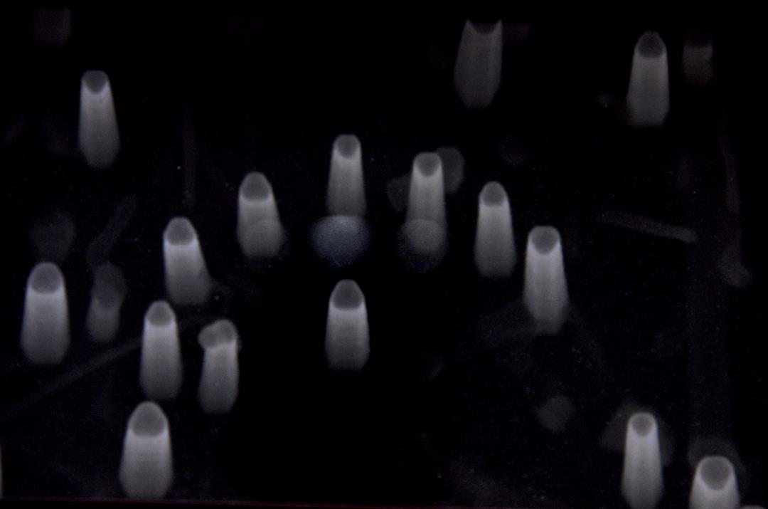
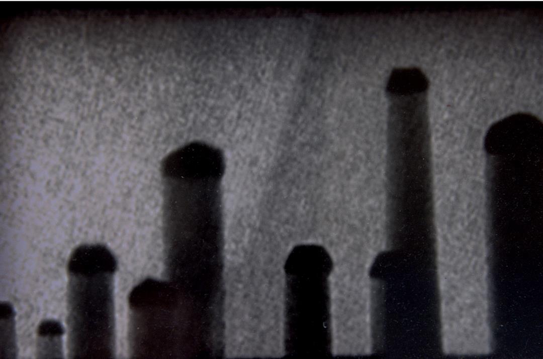
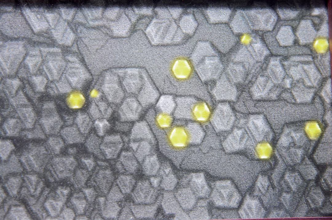
Under a microscope, growing GaP nanowires look like miniature art works. IBM’s Thomas J. Watson Research Center presented Chou with the photos to commemorate her efforts there.
@List.jpg?w=522&h=410&mode=crop&format=webp&quality=80)


@List.jpg?w=522&h=410&mode=crop&format=webp&quality=80)